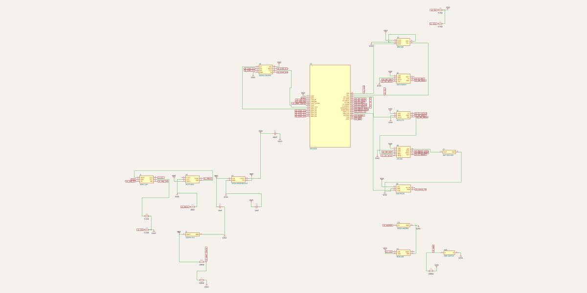
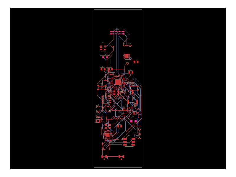
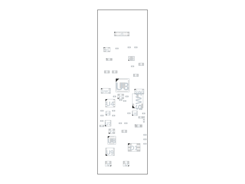
Power along the bottom left, the microcontroller in the middle with every bus leaving its right side, sensors and radio in a column on the right. Arranged to read the same way the system block diagram does.
Netlist
The same information as text. This is the form to review a change in, because it diffs.
COMPONENTS:
 - J1: USB4085-GF-A
 - R1: 5.1kΩ res0402 resistor
 - R2: 5.1kΩ res0402 resistor
 - U1: MCP73831, sot23_5
 - R3: 10kΩ res0402 resistor
 - J2: S2B-PH-K-S, jst_ph_2
 - U2: TPS63001
 - L2: L2, source_component
 - C1: 10uF cap0805 capacitor
 - C2: 22uF cap0805 capacitor
 - U3: RP2350A
 - C3: 100nF cap0402 capacitor
 - Y1: ABM8-272-T3
 - C4: 15pF cap0402 capacitor
 - C11: 100nF cap0402 capacitor
 - C12: 1uF cap0603 capacitor
 - C8: 100nF cap0402 capacitor
 - C9: 2.2uF cap0603 capacitor
 - C10: 10nF cap0402 capacitor
 - C6: 100nF cap0402 capacitor
 - C7: 100nF cap0402 capacitor
 - C5: 15pF cap0402 capacitor
 - R13: 1kΩ res0402 resistor
 - U4: W25Q128JVSIQ, soic8
 - U5: BMP390
 - R4: 4.7kΩ res0402 resistor
 - R5: 4.7kΩ res0402 resistor
 - U6: ICM-42688-P
 - U7: ADXL375
 - U8: SX1262
 - Y2: XTAL-32M-10PF
 - L3: L3, source_component
 - J3: U.FL-R-SMT-1(10)
 - U9: MAX-M10S
 - J5: U.FL-R-SMT-1(10)
 - LS1: PKLCS1212E4001-R1, pinrow2
 - D1: RGB-LED-CC, led5050
 - SW1: JS102011SCQN
 - R6: 100kΩ res0402 resistor
 - SW2: B3U-1000P, smdpushbutton
 - SW3: B3U-1000P, smdpushbutton
 - R10: 330Ω res0402 resistor
 - R11: 220Ω res0402 resistor
 - R12: 220Ω res0402 resistor
 - R9: 10kΩ res0402 resistor
 - J4: SWD-PADS
 - R7: 100kΩ res0402 resistor
 - R8: 100kΩ res0402 resistor
 - L1: L1, source_component

NET: U3_RUN
  - R9 pin2
  - SW3 A2
  - SW3 A1
  - U3 RUN

NET: U3_SWCLK
  - J4 SWCLK
  - U3 SWCLK

NET: U3_SWDIO
  - J4 SWDIO
  - U3 SWDIO

NET: U1_VDD
  - J1 pin10
  - J1 pin15
  - J1 pin7
  - J1 pin2
  - U1 VDD

NET: R1_pos
  - J1 pin3
  - R1 pin1

NET: R2_pos
  - J1 pin14
  - R2 pin1

NET: U1_PROG
  - U1 PROG
  - R3 pin1

NET: U3_USB_DP
  - J1 pin13
  - J1 pin4
  - U3 USB_DP

NET: U3_USB_DM
  - J1 pin12
  - J1 pin5
  - U3 USB_DM

NET: U3_QSPI_SCK
  - U3 QSPI_SCK
  - U4 CLK

NET: U3_QSPI_CS
  - SW2 A2
  - SW2 A1
  - U3 QSPI_CS
  - U4 CS

NET: U4_DI
  - U3 QSPI_D0
  - U4 DI

NET: U4_DO
  - U3 QSPI_D1
  - U4 DO

NET: U4_WP
  - U3 QSPI_D2
  - U4 WP

NET: U4_HOLD
  - U3 QSPI_D3
  - U4 HOLD

NET: U3_SDA
  - U3 SDA
  - U5 SDA
  - R4 pin1

NET: U3_SCL
  - U3 SCL
  - U5 SCL
  - R5 pin1

NET: U3_CS_IMU
  - U3 CS_IMU
  - U6 CS

NET: U3_CS_HIGHG
  - U3 CS_HIGHG
  - U7 CS

NET: U6_SCLK
  - U3 SPI_SCK
  - U6 SCLK
  - U7 SCLK
  - U8 SCK

NET: U3_SPI_MOSI
  - U3 SPI_MOSI
  - U6 SDI
  - U7 SDI
  - U8 MOSI

NET: U3_SPI_MISO
  - U3 SPI_MISO
  - U6 SDO
  - U7 SDO
  - U8 MISO

NET: U3_CS_RADIO
  - U3 CS_RADIO
  - U8 NSS

NET: U3_RADIO_BUSY
  - U3 RADIO_BUSY
  - U8 BUSY

NET: U3_RADIO_DIO1
  - U3 RADIO_DIO1
  - U8 DIO1

NET: U3_RADIO_NRESET
  - U3 RADIO_NRESET
  - U8 NRESET

NET: U3_RADIO_DIO2
  - U3 RADIO_DIO2
  - U8 DIO2

NET: U3_GNSS_TX
  - U3 GNSS_TX
  - U9 RXD

NET: U3_GNSS_RX
  - U3 GNSS_RX
  - U9 TXD

NET: U3_BUZZER
  - U3 BUZZER
  - LS1 IN

NET: U3_LED_R
  - U3 LED_R
  - R10 pin1

NET: D1_A_R
  - R10 pin2
  - D1 A_R

NET: U3_LED_G
  - U3 LED_G
  - R11 pin1

NET: D1_A_G
  - R11 pin2
  - D1 A_G

NET: U3_LED_B
  - U3 LED_B
  - R12 pin1

NET: D1_A_B
  - R12 pin2
  - D1 A_B

NET: U3_XOUT
  - R13 pin2
  - U3 XOUT

NET: U3_XIN
  - C4 pin1 (+)
  - U3 XIN
  - Y1 XA

NET: Y1_XB
  - C5 pin1 (+)
  - Y1 XB
  - R13 pin1

NET: U8_VREG
  - U8 VREG
  - L3 pin1 (+)

NET: U8_DCC_SW
  - L3 pin2 (-)
  - U8 DCC_SW

NET: U8_XTA
  - U8 XTA
  - Y2 XA

NET: U8_XTB
  - U8 XTB
  - Y2 XB

NET: U9_RF_IN
  - U9 RF_IN
  - J5 SIG

NET: L2_pos
  - U2 L1
  - L2 pin1 (+)

NET: L2_neg
  - U2 L2
  - L2 pin2 (-)

NET: VBAT
  - R7 pin1
  - C1 pin1 (+)
  - U2 VIN
  - J2 VBAT
  - U1 VBAT
  - U2 VINA
  - U2 EN

NET: U3_ARM
  - R6 pin1
  - SW1 COM
  - U3 ARM

NET: U3_VBAT_SENSE
  - R8 pin1
  - R7 pin2
  - U3 VBAT_SENSE

NET: U3_VREG_LX
  - U3 VREG_LX
  - L1 pin1 (+)

NET: VCORE
  - U3 DVDD3
  - U3 DVDD2
  - U3 DVDD1
  - U3 VREG_FB
  - L1 pin2 (-)

NET: V3V3
  - U3 VREG_VIN
  - U3 VREG_AVDD
  - U3 USB_OTP_VDD
  - U3 QSPI_IOVDD
  - U3 ADC_AVDD
  - U3 IOVDD6
  - U3 IOVDD5
  - U3 IOVDD4
  - U3 IOVDD3
  - U3 IOVDD2
  - U2 FB
  - R6 pin2
  - U9 V_BCKP
  - U9 V_IO
  - U9 VCC
  - U8 VDD_IN
  - U8 VBAT_IO
  - U8 VBAT
  - C12 pin1 (+)
  - C11 pin1 (+)
  - U7 RESV3
  - U7 VDDIO
  - U7 VS
  - C10 pin1 (+)
  - C9 pin1 (+)
  - C8 pin1 (+)
  - U6 VDDIO
  - U6 VDD
  - R5 pin2
  - R4 pin2
  - C7 pin1 (+)
  - C6 pin1 (+)
  - U5 CSB
  - U5 VDDIO
  - U5 VDD
  - U4 VCC
  - C3 pin1 (+)
  - U3 VDD
  - U2 VOUT
  - C2 pin1 (+)
  - R9 pin1

NET: GND
  - U3 VREG_PGND
  - U2 EPAD
  - U2 PGND
  - U2 PSSYNC
  - J5 GND2
  - J5 GND
  - Y2 CASE2
  - Y2 CASE1
  - C12 pin2 (-)
  - C11 pin2 (-)
  - C10 pin2 (-)
  - C9 pin2 (-)
  - C8 pin2 (-)
  - C7 pin2 (-)
  - C6 pin2 (-)
  - Y1 CASE2
  - Y1 CASE1
  - C5 pin2 (-)
  - C4 pin2 (-)
  - U5 SDO
  - R8 pin2
  - SW1 T1
  - D1 K_B
  - D1 K_G
  - D1 K_R
  - LS1 GND
  - U9 GND12
  - U9 GND10
  - U9 GND1
  - J3 GND2
  - J3 GND
  - U8 EPAD
  - U8 GND20
  - U8 GND8
  - U8 GND5
  - U8 GND2
  - U7 RESV11
  - U7 GND5
  - U7 GND4
  - U7 GND2
  - U6 RESV11
  - U6 RESV10
  - U6 RESV3
  - U6 RESV2
  - U6 RESV7
  - U6 GND
  - U5 VSS9
  - U5 VSS8
  - U5 VSS3
  - U4 GND
  - C3 pin2 (-)
  - U3 GND
  - C2 pin2 (-)
  - C1 pin2 (-)
  - U2 GND
  - J2 GND
  - R3 pin2
  - U1 VSS
  - R2 pin2
  - R1 pin2
  - J1 pin20
  - J1 pin19
  - J1 pin18
  - J1 pin17
  - J1 pin9
  - J1 pin16
  - J1 pin8
  - J1 pin1
  - J4 GND
  - SW3 B2
  - SW3 B1
  - SW2 B2
  - SW2 B1


COMPONENT_PINS:
J1 (USB4085-GF-A)
- pin1(A1): NETS(GND)
- pin2(A4): NETS(U1_VDD)
- pin3(A5): NETS(R1_pos)
- pin4(A6): NETS(U3_USB_DP)
- pin5(A7): NETS(U3_USB_DM)
- pin6(A8): NOT_CONNECTED
- pin7(A9): NETS(U1_VDD)
- pin8(A12): NETS(GND)
- pin9(B12): NETS(GND)
- pin10(B9): NETS(U1_VDD)
- pin11(B8): NOT_CONNECTED
- pin12(B7): NETS(U3_USB_DM)
- pin13(B6): NETS(U3_USB_DP)
- pin14(B5): NETS(R2_pos)
- pin15(B4): NETS(U1_VDD)
- pin16(B1): NETS(GND)
- pin17(SHELL00): NETS(GND)
- pin18(SHELL01): NETS(GND)
- pin19(SHELL10): NETS(GND)
- pin20(SHELL11): NETS(GND)

R1 (5.1kΩ res0402)
- pin1(anode, pos, left): NETS(R1_pos)
- pin2(cathode, neg, right): NETS(GND)

R2 (5.1kΩ res0402)
- pin1(anode, pos, left): NETS(R2_pos)
- pin2(cathode, neg, right): NETS(GND)

U1 (MCP73831)
- pin1(STAT): NOT_CONNECTED
- pin2(VSS): NETS(GND)
- pin3(VBAT): NETS(VBAT)
- pin4(VDD): NETS(U1_VDD)
- pin5(PROG): NETS(U1_PROG)

R3 (10kΩ res0402)
- pin1(anode, pos, left): NETS(U1_PROG)
- pin2(cathode, neg, right): NETS(GND)

J2 (S2B-PH-K-S)
- pin1(VBAT): NETS(VBAT)
- pin2(GND): NETS(GND)

U2 (TPS63001)
- pin1(VOUT): NETS(V3V3)
- pin2(L2): NETS(L2_neg)
- pin3(PGND): NETS(GND)
- pin4(L1): NETS(L2_pos)
- pin5(VIN): NETS(VBAT)
- pin6(EN): NETS(VBAT)
- pin7(PSSYNC): NETS(GND)
- pin8(VINA): NETS(VBAT)
- pin9(GND): NETS(GND)
- pin10(FB): NETS(V3V3)
- pin11(EPAD): NETS(GND)

L2
- pin1(anode, pos, left): NETS(L2_pos)
- pin2(cathode, neg, right): NETS(L2_neg)

C1 (10uF cap0805)
- pin1(pos, anode, left): NETS(VBAT)
- pin2(neg, cathode, right): NETS(GND)

C2 (22uF cap0805)
- pin1(pos, anode, left): NETS(V3V3)
- pin2(neg, cathode, right): NETS(GND)

U3 (RP2350A)
- pin1(VDD): NETS(V3V3)
- pin2(GPIO0): NOT_CONNECTED
- pin3(GPIO1): NOT_CONNECTED
- pin4(GPIO2): NOT_CONNECTED
- pin5(GPIO3): NOT_CONNECTED
- pin6(DVDD1): NETS(VCORE)
- pin7(SDA): NETS(U3_SDA)
- pin8(SCL): NETS(U3_SCL)
- pin9(GPIO6): NOT_CONNECTED
- pin10(GPIO7): NOT_CONNECTED
- pin11(IOVDD2): NETS(V3V3)
- pin12(GPIO8): NOT_CONNECTED
- pin13(LED_B): NETS(U3_LED_B)
- pin14(GPIO10): NOT_CONNECTED
- pin15(GPIO11): NOT_CONNECTED
- pin16(LED_G): NETS(U3_LED_G)
- pin17(ARM): NETS(U3_ARM)
- pin18(BUZZER): NETS(U3_BUZZER)
- pin19(LED_R): NETS(U3_LED_R)
- pin20(IOVDD3): NETS(V3V3)
- pin21(XIN): NETS(U3_XIN)
- pin22(XOUT): NETS(U3_XOUT)
- pin23(DVDD2): NETS(VCORE)
- pin24(SWCLK): NETS(U3_SWCLK)
- pin25(SWDIO): NETS(U3_SWDIO)
- pin26(RUN): NETS(U3_RUN)
- pin27(SPI_MISO): NETS(U3_SPI_MISO)
- pin28(CS_IMU): NETS(U3_CS_IMU)
- pin29(SPI_SCK): NETS(U6_SCLK)
- pin30(IOVDD4): NETS(V3V3)
- pin31(SPI_MOSI): NETS(U3_SPI_MOSI)
- pin32(CS_HIGHG): NETS(U3_CS_HIGHG)
- pin33(CS_RADIO): NETS(U3_CS_RADIO)
- pin34(RADIO_BUSY): NETS(U3_RADIO_BUSY)
- pin35(RADIO_DIO1): NETS(U3_RADIO_DIO1)
- pin36(GNSS_TX): NETS(U3_GNSS_TX)
- pin37(GNSS_RX): NETS(U3_GNSS_RX)
- pin38(IOVDD5): NETS(V3V3)
- pin39(DVDD3): NETS(VCORE)
- pin40(VBAT_SENSE): NETS(U3_VBAT_SENSE)
- pin41(RADIO_NRESET): NETS(U3_RADIO_NRESET)
- pin42(RADIO_DIO2): NETS(U3_RADIO_DIO2)
- pin43(GPIO29): NOT_CONNECTED
- pin44(ADC_AVDD): NETS(V3V3)
- pin45(IOVDD6): NETS(V3V3)
- pin46(VREG_AVDD): NETS(V3V3)
- pin47(VREG_PGND): NETS(GND)
- pin48(VREG_LX): NETS(U3_VREG_LX)
- pin49(VREG_VIN): NETS(V3V3)
- pin50(VREG_FB): NETS(VCORE)
- pin51(USB_DM): NETS(U3_USB_DM)
- pin52(USB_DP): NETS(U3_USB_DP)
- pin53(USB_OTP_VDD): NETS(V3V3)
- pin54(QSPI_IOVDD): NETS(V3V3)
- pin55(QSPI_D3): NETS(U4_HOLD)
- pin56(QSPI_SCK): NETS(U3_QSPI_SCK)
- pin57(QSPI_D0): NETS(U4_DI)
- pin58(QSPI_D2): NETS(U4_WP)
- pin59(QSPI_D1): NETS(U4_DO)
- pin60(QSPI_CS): NETS(U3_QSPI_CS)
- pin61(GND): NETS(GND)

C3 (100nF cap0402)
- pin1(pos, anode, left): NETS(V3V3)
- pin2(neg, cathode, right): NETS(GND)

Y1 (ABM8-272-T3)
- pin1(XA): NETS(U3_XIN)
- pin2(CASE1): NETS(GND)
- pin3(XB): NETS(Y1_XB)
- pin4(CASE2): NETS(GND)

C4 (15pF cap0402)
- pin1(pos, anode, left): NETS(U3_XIN)
- pin2(neg, cathode, right): NETS(GND)

C11 (100nF cap0402)
- pin1(pos, anode, left): NETS(V3V3)
- pin2(neg, cathode, right): NETS(GND)

C12 (1uF cap0603)
- pin1(pos, anode, left): NETS(V3V3)
- pin2(neg, cathode, right): NETS(GND)

C8 (100nF cap0402)
- pin1(pos, anode, left): NETS(V3V3)
- pin2(neg, cathode, right): NETS(GND)

C9 (2.2uF cap0603)
- pin1(pos, anode, left): NETS(V3V3)
- pin2(neg, cathode, right): NETS(GND)

C10 (10nF cap0402)
- pin1(pos, anode, left): NETS(V3V3)
- pin2(neg, cathode, right): NETS(GND)

C6 (100nF cap0402)
- pin1(pos, anode, left): NETS(V3V3)
- pin2(neg, cathode, right): NETS(GND)

C7 (100nF cap0402)
- pin1(pos, anode, left): NETS(V3V3)
- pin2(neg, cathode, right): NETS(GND)

C5 (15pF cap0402)
- pin1(pos, anode, left): NETS(Y1_XB)
- pin2(neg, cathode, right): NETS(GND)

R13 (1kΩ res0402)
- pin1(anode, pos, left): NETS(Y1_XB)
- pin2(cathode, neg, right): NETS(U3_XOUT)

U4 (W25Q128JVSIQ)
- pin1(CS): NETS(U3_QSPI_CS)
- pin2(DO): NETS(U4_DO)
- pin3(WP): NETS(U4_WP)
- pin4(GND): NETS(GND)
- pin5(DI): NETS(U4_DI)
- pin6(CLK): NETS(U3_QSPI_SCK)
- pin7(HOLD): NETS(U4_HOLD)
- pin8(VCC): NETS(V3V3)

U5 (BMP390)
- pin1(VDDIO): NETS(V3V3)
- pin2(SCL): NETS(U3_SCL)
- pin3(VSS3): NETS(GND)
- pin4(SDA): NETS(U3_SDA)
- pin5(SDO): NETS(GND)
- pin6(CSB): NETS(V3V3)
- pin7(INT): NOT_CONNECTED
- pin8(VSS8): NETS(GND)
- pin9(VSS9): NETS(GND)
- pin10(VDD): NETS(V3V3)

R4 (4.7kΩ res0402)
- pin1(anode, pos, left): NETS(U3_SDA)
- pin2(cathode, neg, right): NETS(V3V3)

R5 (4.7kΩ res0402)
- pin1(anode, pos, left): NETS(U3_SCL)
- pin2(cathode, neg, right): NETS(V3V3)

U6 (ICM-42688-P)
- pin1(SDO): NETS(U3_SPI_MISO)
- pin2(RESV2): NETS(GND)
- pin3(RESV3): NETS(GND)
- pin4(INT1): NOT_CONNECTED
- pin5(VDDIO): NETS(V3V3)
- pin6(GND): NETS(GND)
- pin7(RESV7): NETS(GND)
- pin8(VDD): NETS(V3V3)
- pin9(INT2): NOT_CONNECTED
- pin10(RESV10): NETS(GND)
- pin11(RESV11): NETS(GND)
- pin12(CS): NETS(U3_CS_IMU)
- pin13(SCLK): NETS(U6_SCLK)
- pin14(SDI): NETS(U3_SPI_MOSI)

U7 (ADXL375)
- pin1(VDDIO): NETS(V3V3)
- pin2(GND2): NETS(GND)
- pin3(RESV3): NETS(V3V3)
- pin4(GND4): NETS(GND)
- pin5(GND5): NETS(GND)
- pin6(VS): NETS(V3V3)
- pin7(CS): NETS(U3_CS_HIGHG)
- pin8(INT1): NOT_CONNECTED
- pin9(INT2): NOT_CONNECTED
- pin10(NC): NOT_CONNECTED
- pin11(RESV11): NETS(GND)
- pin12(SDO): NETS(U3_SPI_MISO)
- pin13(SDI): NETS(U3_SPI_MOSI)
- pin14(SCLK): NETS(U6_SCLK)

U8 (SX1262)
- pin1(VDD_IN): NETS(V3V3)
- pin2(GND2): NETS(GND)
- pin3(XTA): NETS(U8_XTA)
- pin4(XTB): NETS(U8_XTB)
- pin5(GND5): NETS(GND)
- pin6(DIO3): NOT_CONNECTED
- pin7(VREG): NETS(U8_VREG)
- pin8(GND8): NETS(GND)
- pin9(DCC_SW): NETS(U8_DCC_SW)
- pin10(VBAT): NETS(V3V3)
- pin11(VBAT_IO): NETS(V3V3)
- pin12(DIO2): NETS(U3_RADIO_DIO2)
- pin13(DIO1): NETS(U3_RADIO_DIO1)
- pin14(BUSY): NETS(U3_RADIO_BUSY)
- pin15(NRESET): NETS(U3_RADIO_NRESET)
- pin16(MISO): NETS(U3_SPI_MISO)
- pin17(MOSI): NETS(U3_SPI_MOSI)
- pin18(SCK): NETS(U6_SCLK)
- pin19(NSS): NETS(U3_CS_RADIO)
- pin20(GND20): NETS(GND)
- pin21(RFI_P): NOT_CONNECTED
- pin22(RFI_N): NOT_CONNECTED
- pin23(RFO): NOT_CONNECTED
- pin24(VR_PA): NOT_CONNECTED
- pin25(EPAD): NETS(GND)

Y2 (XTAL-32M-10PF)
- pin1(XA): NETS(U8_XTA)
- pin2(CASE1): NETS(GND)
- pin3(XB): NETS(U8_XTB)
- pin4(CASE2): NETS(GND)

L3
- pin1(anode, pos, left): NETS(U8_VREG)
- pin2(cathode, neg, right): NETS(U8_DCC_SW)

J3 (U.FL-R-SMT-1(10))
- pin1(ANT): NOT_CONNECTED
- pin2(GND): NETS(GND)
- pin3(GND2): NETS(GND)

U9 (MAX-M10S)
- pin1(GND1): NETS(GND)
- pin2(TXD): NETS(U3_GNSS_RX)
- pin3(RXD): NETS(U3_GNSS_TX)
- pin4(TIMEPULSE): NOT_CONNECTED
- pin5(EXTINT): NOT_CONNECTED
- pin6(V_BCKP): NETS(V3V3)
- pin7(V_IO): NETS(V3V3)
- pin8(VCC): NETS(V3V3)
- pin9(RESET_N): NOT_CONNECTED
- pin10(GND10): NETS(GND)
- pin11(RF_IN): NETS(U9_RF_IN)
- pin12(GND12): NETS(GND)
- pin13(LNA_EN): NOT_CONNECTED
- pin14(VCC_RF): NOT_CONNECTED
- pin15(VIO_SEL): NOT_CONNECTED
- pin16(SDA): NOT_CONNECTED
- pin17(SCL): NOT_CONNECTED
- pin18(SAFEBOOT_N): NOT_CONNECTED

J5 (U.FL-R-SMT-1(10))
- pin1(SIG): NETS(U9_RF_IN)
- pin2(GND): NETS(GND)
- pin3(GND2): NETS(GND)

LS1 (PKLCS1212E4001-R1)
- pin1(IN): NETS(U3_BUZZER)
- pin2(GND): NETS(GND)

D1 (RGB-LED-CC)
- pin1(A_B): NETS(D1_A_B)
- pin2(K_B): NETS(GND)
- pin3(A_R): NETS(D1_A_R)
- pin4(K_R): NETS(GND)
- pin5(A_G): NETS(D1_A_G)
- pin6(K_G): NETS(GND)

SW1 (JS102011SCQN)
- pin1(T1): NETS(GND)
- pin2(COM): NETS(U3_ARM)
- pin3(T3): NOT_CONNECTED

R6 (100kΩ res0402)
- pin1(anode, pos, left): NETS(U3_ARM)
- pin2(cathode, neg, right): NETS(V3V3)

SW2 (B3U-1000P)
- pin1(A1): NETS(U3_QSPI_CS)
- pin2(A2): NETS(U3_QSPI_CS)
- pin3(B1): NETS(GND)
- pin4(B2): NETS(GND)

SW3 (B3U-1000P)
- pin1(A1): NETS(U3_RUN)
- pin2(A2): NETS(U3_RUN)
- pin3(B1): NETS(GND)
- pin4(B2): NETS(GND)

R10 (330Ω res0402)
- pin1(anode, pos, left): NETS(U3_LED_R)
- pin2(cathode, neg, right): NETS(D1_A_R)

R11 (220Ω res0402)
- pin1(anode, pos, left): NETS(U3_LED_G)
- pin2(cathode, neg, right): NETS(D1_A_G)

R12 (220Ω res0402)
- pin1(anode, pos, left): NETS(U3_LED_B)
- pin2(cathode, neg, right): NETS(D1_A_B)

R9 (10kΩ res0402)
- pin1(anode, pos, left): NETS(V3V3)
- pin2(cathode, neg, right): NETS(U3_RUN)

J4 (SWD-PADS)
- pin1(SWCLK): NETS(U3_SWCLK)
- pin2(SWDIO): NETS(U3_SWDIO)
- pin3(GND): NETS(GND)

R7 (100kΩ res0402)
- pin1(anode, pos, left): NETS(VBAT)
- pin2(cathode, neg, right): NETS(U3_VBAT_SENSE)

R8 (100kΩ res0402)
- pin1(anode, pos, left): NETS(U3_VBAT_SENSE)
- pin2(cathode, neg, right): NETS(GND)

L1
- pin1(anode, pos, left): NETS(U3_VREG_LX)
- pin2(cathode, neg, right): NETS(VCORE)